Keithley 615 Electrometer Interface - Part 1: Replacement PCBs
This is a project that I started a bit over a year ago, though which is still in progress at the time of writing. There are two GitHub repos associated with it:
- PCB designs: https://github.com/farlepet/keithley-615-printer-boards
- Firmware: https://github.com/farlepet/keithley-615-net-fw
Background
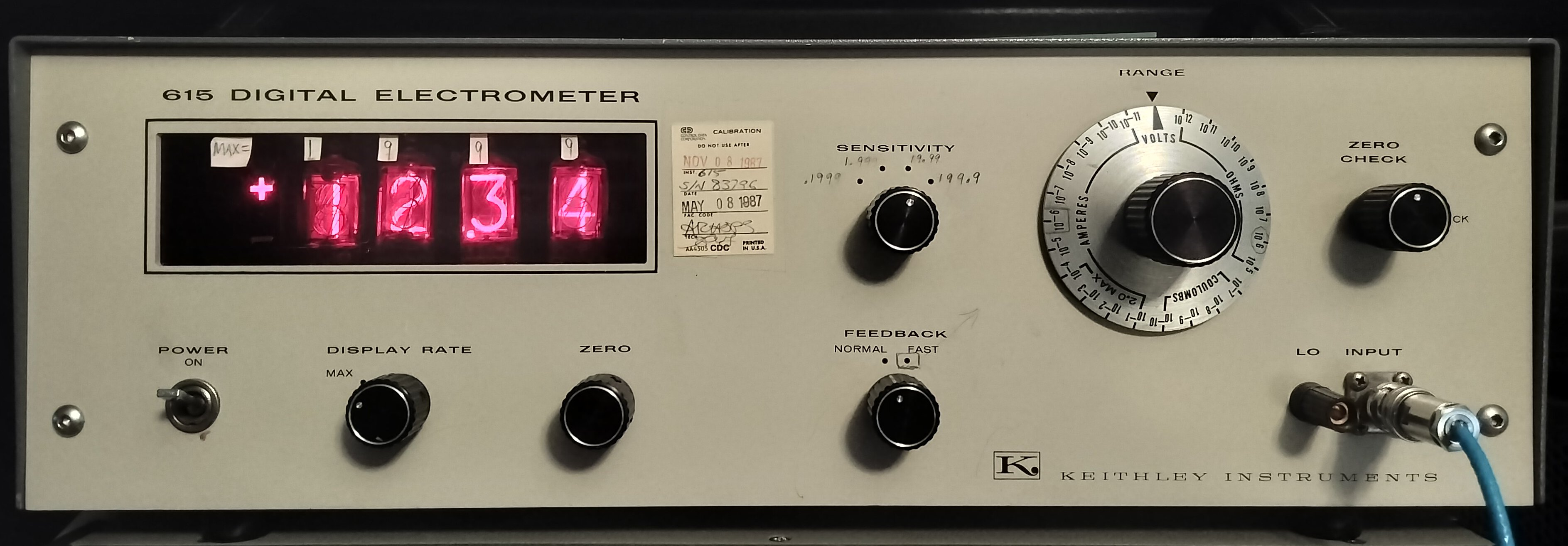
Several years ago, I came across a Keithley 615 electrometer that was being thrown out by my university, along with several other items from the physics and biology departments. It also came with its origional manual, which is nice. (Though mediocre scans of the manual are also available online - basically the only mention of this instrument I could find).
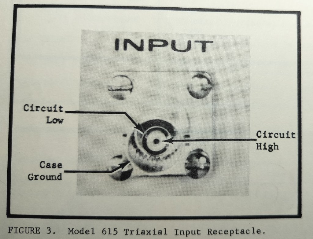
For quite a while it just sat gathering dust. About a year ago I deceded to finally take a look at it. Of course, this doesn’t use banana connectors like your standard multimeter, but rather a tri-axial BNC connector. I’m pretty sure I tried to force a standard BNC cable to make with this connector back when I first got it, and that didn’t work properly, which is probably why I never used it. Looking at the manual, this makes sense, since while the inner pin is the positive as you would expect, the outer conductor is chassis ground used for shielding, not the negative. The negative connector was the ring in-between the center pin and the outer shield.
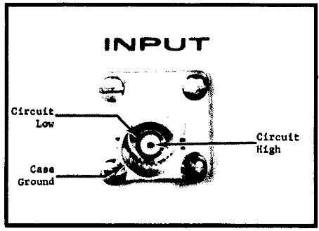
Note: I’m using the low-quality 1-bit color scans from Tektronix where possible, as I don’t have a functioning scanner at the moment. The above is a pretty eggregious example of the quality loss, here is the same figure in the physical manual:
I was able to test it by applying a voltage via some wires to the proper contacts in the connector, though ultimately I had to end up buying a triax to BNC adapter cable (and these aren’t cheap, plus the connector I ended up getting actually had three bayonet locking tabs on it for new instruments, rather than the two my instrument had, so I had to file one off to make it work). For initial “calibration” (using a low-accuracy power supply along with a decent multimeter I had at the time), I just supplied the input inside the instrument, at the other side of the coax.
The version of the manual I had unfortunately did not have the “Servicing” or “Calibration” sections, but the Tektronix scan did. Overall, it was actually one of the easiest calibrations I have done. Part of this is probably due to the lack of need to accurately calibrate the zero point - the instrument has a zero control on the front (and a coarse zero at the rear) that can be fine-tuned each time it is used.
While I was working on it, I noticed that it was missing two cards, and was also curious about the “PRINTER/CONTROL” connector at the back. Looking through the manual, this connector provided the current reading of the instrument and it’s current settings as BCD (binary-coded decimal), and the two missing cards were buffers along with some “data ready” logic. And of course, being that this was from the early- to mid-seventies (based on the date codes on the chips, most from 1971, one from 1973), the manual also had full schematics for the entire instrument, including these optional cards, along with the entire theory of operation for all aspects of the instrument.
(As an aside, I love how the manual has a section on replacable parts, in which it lists every component in the system. That is in contrast to most modern devices that simply state that the contain no “user servicable parts.”)
When I saw this, I had a somewhat irrational thought: I wanted to build new versions of these boards (PC218 and PC209), and create a communication adapter that would utilize that port. So I spent the next couple days designing the replacement boards in KiCAD. I had to first create a part/footprint for the card-edge connectors, as they were non-standard and the tab was in different places on both boards. To confirm I got the spacing and size correct before ordering the boards, I exported them as an STL and 3D-printed them first (I have since thrown these out, and didn’t take any pictures).
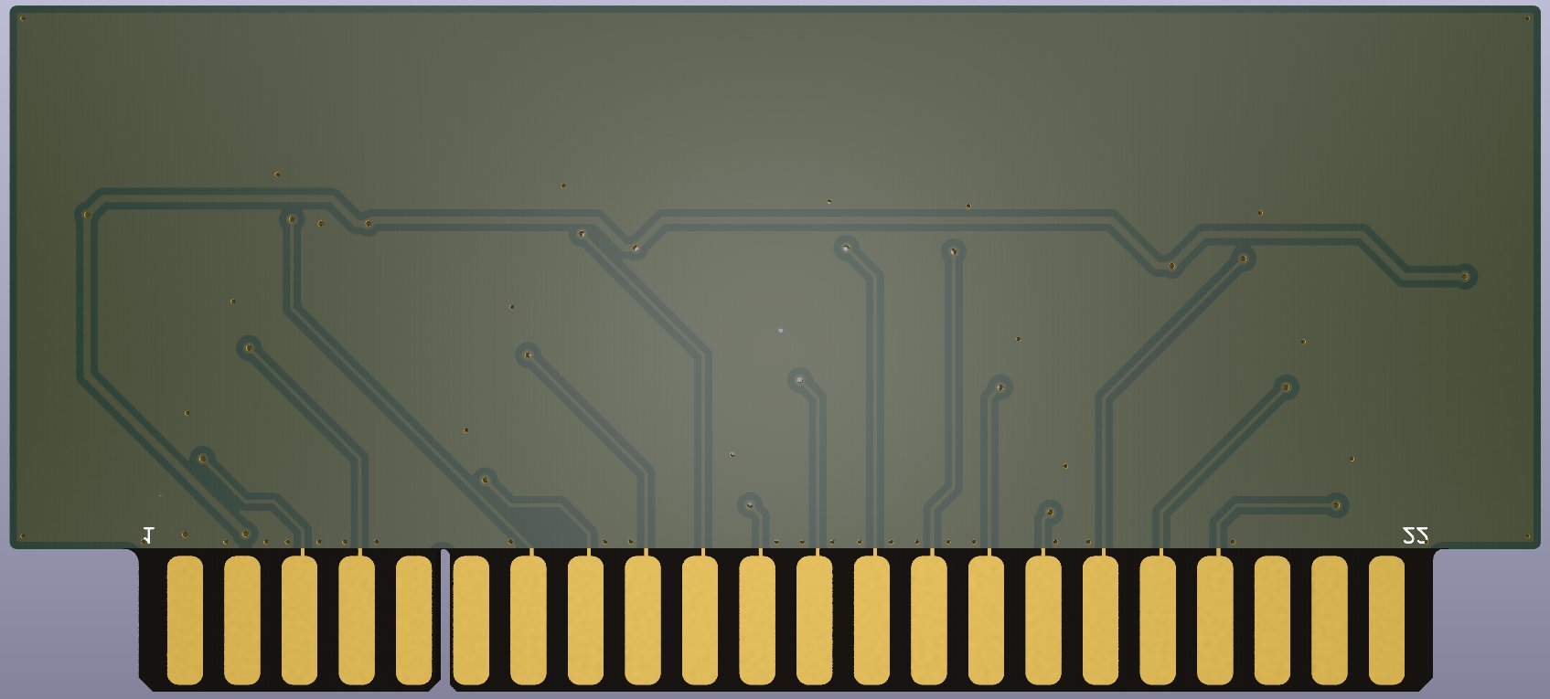
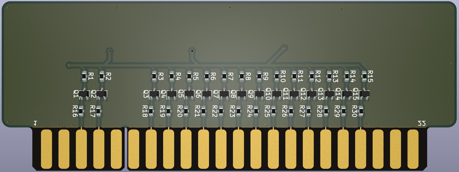
PC218
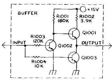
PC218 was just a bunch of inverting buffers made from discrete NPN transistors. The first transistor acted as a simple inverter, then the next two transistors acted as the lower-impedance (low impedance when pulling low, ~3.9 K when pulling high) output buffer.
I made two versions of this board - v1 used the exact same implementation, with discrete transistor inverting buffers, though with more modern SMD components. v2 still used an NPN transistor for the inverting stage (it was cheaper than getting an inverter IC), but then used a 4010 buffer for the output stage. This version won’t have the exact same output characteristics of the first version and the original, but really it should actually perform better as long the attached equipment isn’t counting on the 3.9k pull-up resistor. I haven’t seen a single example of a commercial product that connects to this port, apart from the Model 4405 “Terminal Box” that Keithley sold, so it’s possible that anything that was ever used with that port was home-built (but again, I can barely find anything about this instrument online apart from the manual).
| Ver | Front | Rear |
|---|---|---|
| V1.0 | 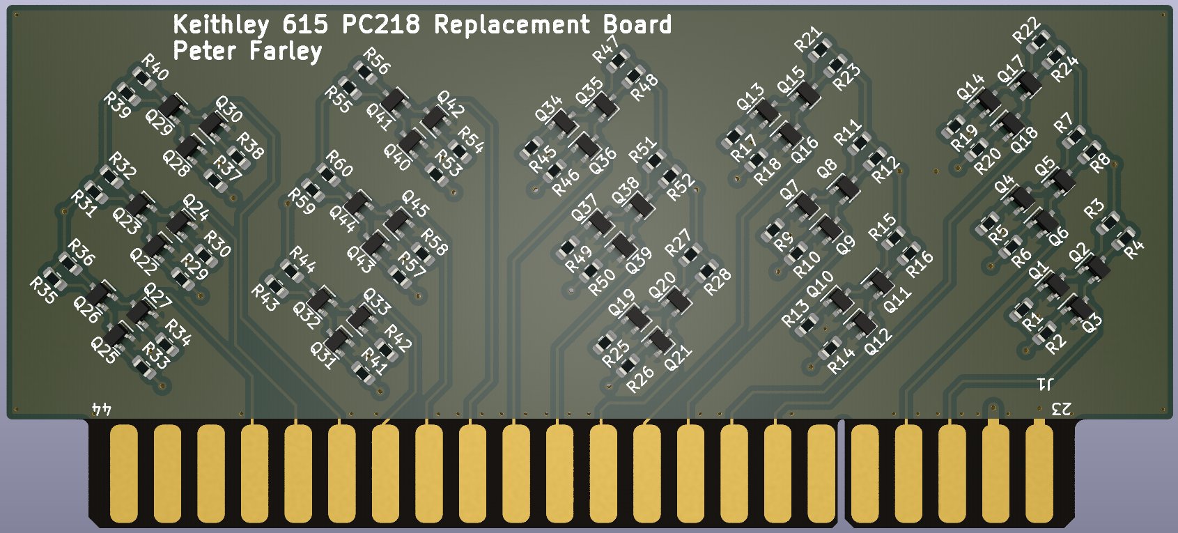 |
 |
| v2.0 | 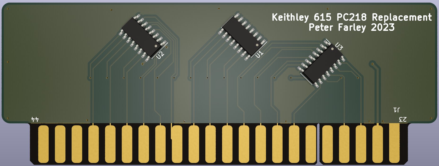 |
 |
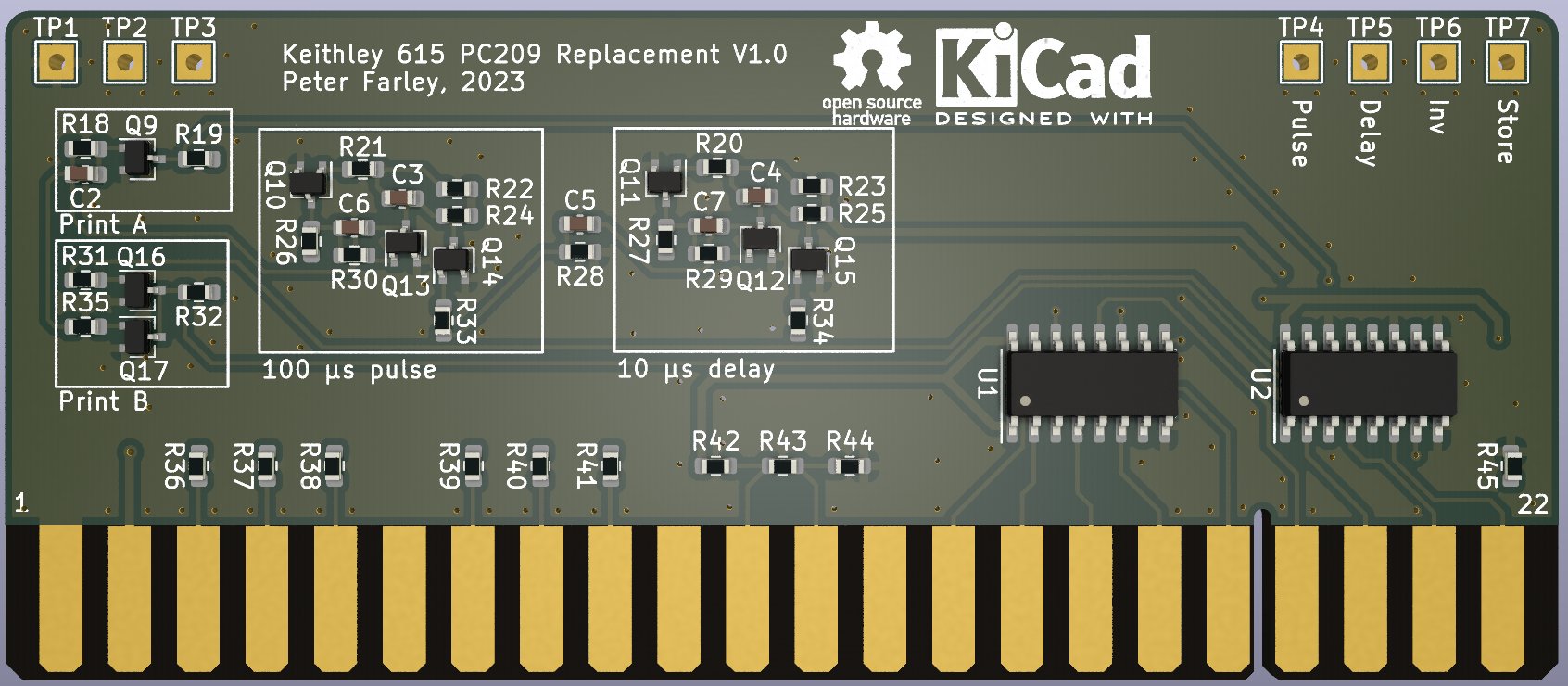
PC209
PC209 was more complicated. It still consisted mainly of inverting buffer blocks, but it also had some logic in the form of two MC724P quad NOR gates. It wasn’t super easy to find a good datasheet for these parts - most of the search results are of people/companies selling these chips, and the few datasheet sites that come up don’t actually have anything, though one did have a databook excerpt that covered a similar chip, the MC824 and MC924. These at least told me it was probably in Motorola’s MRTL family. After some searching, I finally found the correct databook on bitsavers. Interestingly, these were simply refered to as “Quad 2-Input Gate” chips, not NOR gates, while all the other logic gates were identified by the gate type. I suspect that this was due to them being “fundamental” logic gates that can build any other logic (the Apollo AGC exclusively used NOR chips, for instance), and maybe this was much more common than the NAND gate for such purposes.
Anyway, the main reason I wanted some more details on the NOR gates used in this board, is that I wanted to see if I could find a modern replacement, as these gates were used as a part of a delay- and pulse-generation circuit:
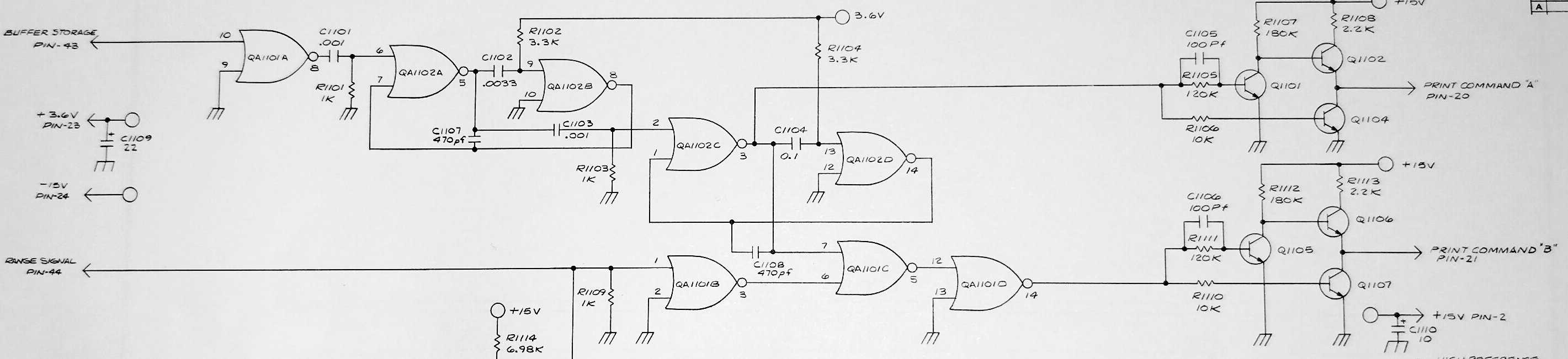
Of course, nobody makes RTL (Resistor-Transistor Logic) chips these days, so I had to end up re-designing it anyway. Initially I looked into using something like a 556 or some other timer chip to implement this functionality, but it turned out to be ill-suited for the task. In the end, I ended up re-designing it from discrete transistors. I chose discrete transistors partially so that I could simulate the delay and pulse-width with Qucs-S + XYCE and tune the component values accordingly (the expected values are specified in the manual). Essentially it was just a re-implementation of the RTL logic using discrete components, rather than a full redesign:
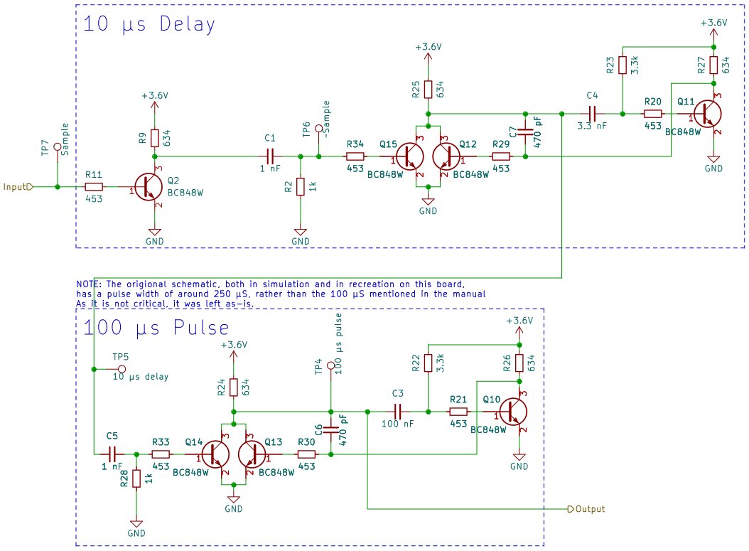
Apart from the timing portion, I used the same inverting buffer design as the v2 PC209 replacement boards.
| Front | Rear |
|---|---|
 |
 |
To Be Continued
I’m not sure why I got so invested in this instrument, probably a combination of wanting something to work on at the time, and allure of the nixie tubes. Regardless, in the next post (hopefully I won’t procrastinate for months on this one) I’ll write about testing and debugging these boards, and the next steps towards the external interface board.